Chip Breakthrough Cuts AI Energy Use, Boosts Computing Power
A bus-sized machine is etching the world's smallest computer chip features at just eight nanometers, tripling transistor counts while keeping energy use flat. The breakthrough could let AI data centers run three times faster without burning more power.
The world's most precise light beam just solved one of AI's biggest problems: how to keep getting smarter without melting the planet.
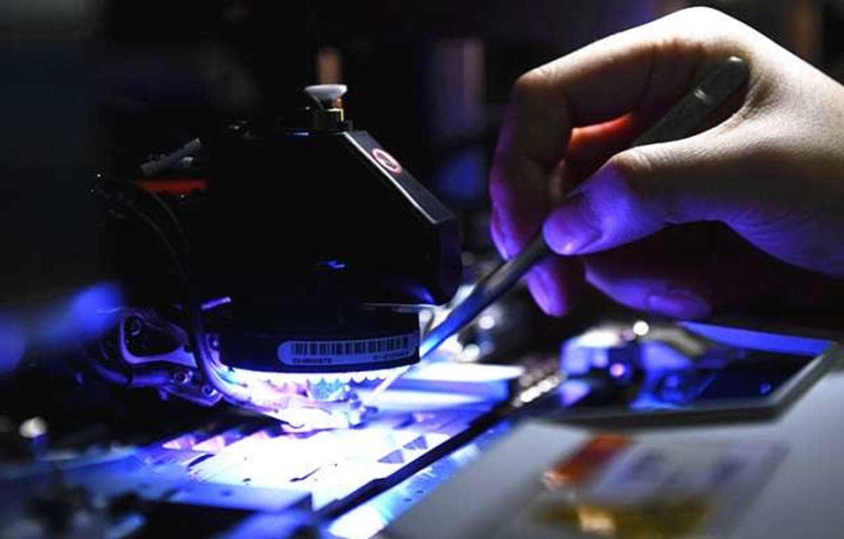
A new extreme ultraviolet light system from Dutch company ASML has etched the smallest chip features ever achieved in a single commercial step. At just eight nanometers wide, these microscopic structures pack nearly three times as many transistors onto a chip as previous designs, all without increasing power consumption.
The machine works by shooting special ultraviolet light through patterned masks onto silicon wafers coated with light-sensitive chemicals. The light hardens the chemicals in precise shapes that become transistors and ultra-fine wiring. What makes this breakthrough special is the light itself: at 13.5 nanometers, its wavelength is so short it gets absorbed by almost everything, including air.
Only mirrors made from nanometer-thin layers of silicon and molybdenum, crafted in Germany, can reflect this finicky light accurately enough. Even atomic-scale imperfections would blur the image and ruin the chip.
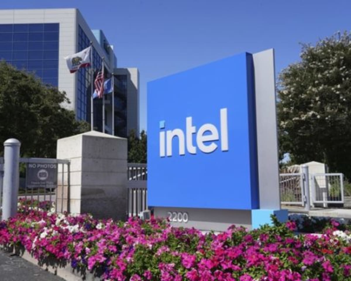
The $400 million machines have already shipped to major chipmakers including Intel and SK hynix. Maarten Voncken, who leads research at ASML, says the urgency is real. "The demands we see are monumental in the number of chips that are needed," he explained at a recent California conference, citing explosive AI growth.
For decades, the semiconductor industry followed Moore's Law, doubling transistor counts every two years. But AI's hunger for computing power has made keeping that pace increasingly hard. Smaller features mean more transistors in the same space, boosting performance without dramatically increasing energy use, exactly what AI data centers desperately need.
The innovation reported in Nature represents decades of patient work. Jeffrey Bokor, an early pioneer of this technology at Bell Labs, remembers when colleagues called it "lunatic fringe" science because controlling such extreme light seemed impossible. Today, powerful lasers, molten-tin plasma sources, and nanometer-precision mirrors have turned that fringe dream into commercial reality.
The Ripple Effect
This breakthrough ripples far beyond faster smartphones. AI models powering language understanding, medical diagnostics, and climate prediction rely on massive computational throughput. Data centers could run far more calculations without additional energy use if chips pack denser transistors, turning what would have required building entire new power plants into a simple chip upgrade.
The technology also opens doors to three-dimensional chip designs, stacking transistors like microscopic skyscrapers to multiply functionality without expanding footprints. Researchers are already exploring these 3D designs at Belgium's Imec research institute, though managing heat from densely packed vertical transistors remains a challenge.
ASML is already developing even more precise machines with higher numerical apertures, continuing to shrink features further. The company calls this next stage "hyper-NA," pushing toward a 0.75 numerical aperture compared to today's 0.55. Beyond that would require switching to X-ray wavelengths, necessitating completely new machine designs.
The innovation bridges scientific ambition and industrial-scale production, moving from experimental laboratories into the heart of global semiconductor supply chains. As AI continues accelerating, advances like ASML's system could redefine not just computing speed and efficiency, but the trajectory of technological development itself.
More Images


Based on reporting by Google News - Tech Breakthrough
This story was written by BrightWire based on verified news reports.
Spread the positivity!
Share this good news with someone who needs it