30 Students Tour Northeast's Chip Innovation Hub
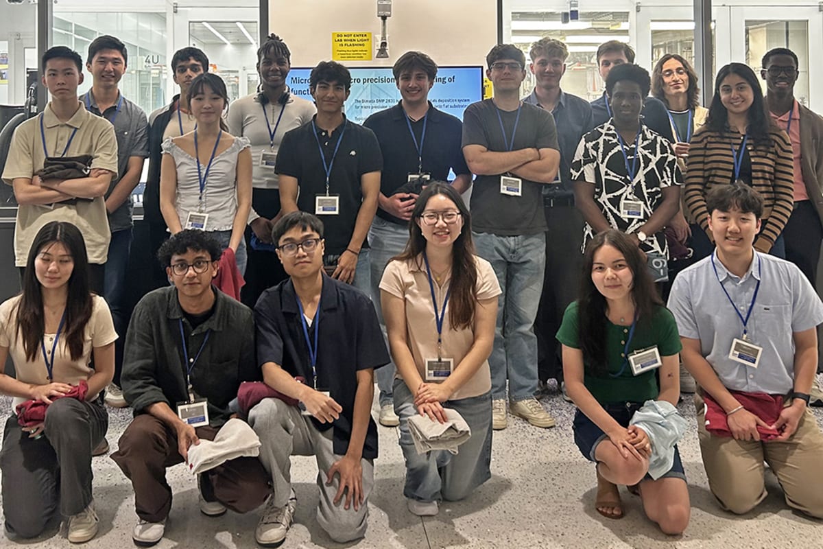
Thirty undergraduate students from across the Northeast spent a week exploring the future of microelectronics, touring cutting-edge facilities from MIT to GlobalFoundries. The immersive program connected classroom learning with real-world innovation in America's semiconductor industry.
Thirty students just got a backstage pass to the technology powering everything from smartphones to quantum computers, and it might have changed their career paths forever.
The Northeast Microelectronics Internship Program brought together undergraduate students from leading universities for an intensive week exploring semiconductor technology. Held in July, the program offered something most engineering students never get: hands-on access to both academic research labs and advanced manufacturing facilities.
Students started at MIT.nano, where they heard from researchers pushing the boundaries of chip design and materials science. Graduate students shared their work on everything from nanoelectronics to quantum technologies, showing participants what cutting-edge research looks like in practice.
The week included tours of IBM Research, where students saw High-NA EUV lithography and quantum hardware development in action. At GlobalFoundries, they donned "bunny suits" to tour a state-of-the-art 300mm semiconductor fabrication facility, witnessing how microscopic circuits are manufactured at scale.
"The externship gave me a behind-the-scenes look at the advanced technologies driving the microelectronics industry while allowing me to connect one-on-one with researchers and industry professionals," says Sean Kim, a Princeton student. His experience mirrors what many participants felt about the program's impact.
An industry panel brought together professionals from companies like Analog Devices and Cadence Design Systems. They shared honest advice about transitioning from academia to careers in semiconductors, helping students understand the many pathways available in the field.
MIT student Shanti Visurakapalli found the combination particularly valuable. "This experience, complemented with the industry panel, gave many of us the perspective we needed to weigh future graduate and professional options," she says.
The program took students to premier institutions including Rensselaer Polytechnic Institute and NY CREATES. At each stop, they connected with engineers, scientists, and researchers who explained how academic breakthroughs become commercial products.
The Ripple Effect
Programs like this do more than inspire individual students. They're building the workforce America needs to lead in semiconductor technology, a field critical to everything from national security to medical devices.
By connecting 30 students with mentors and showing them real opportunities in microelectronics, the program creates ripples that extend far beyond one week. These relationships and insights could guide career decisions for years to come.
The students came from different universities but left with shared connections and a deeper understanding of how microelectronics shapes our world. For many, seeing researchers tackle global challenges through engineering transformed how they think about their own potential impact.
The next generation of chip innovators just got a powerful glimpse of their future.
Based on reporting by MIT News
This story was written by BrightWire based on verified news reports.
Spread the positivity!
Share this good news with someone who needs it