Cornell Scientists See Atoms Inside Computer Chips
Researchers can now see atomic-scale defects inside computer chips for the first time, revealing tiny flaws that slow down electronics. The breakthrough could help make everything from smartphones to AI systems work better.
Scientists at Cornell University just achieved something that sounds impossible: they can now see individual atoms inside the tiny transistors that power our phones, cars, and computers.
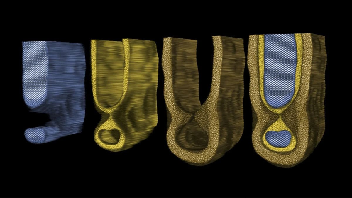
Using an advanced electron microscopy technique, the research team mapped the exact positions of atoms in computer chip channels that are only 15 to 18 atoms wide. What they found surprised them: small defects they nicknamed "mouse bites" that form during manufacturing and disrupt how electrons flow through chips.
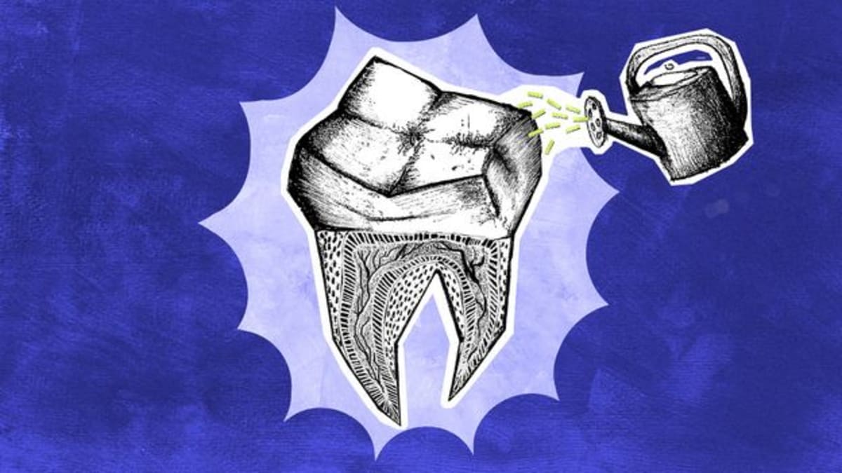
"The transistor is like a little pipe for electrons instead of water," explained David Muller, who led the Cornell project. "If the walls of the pipe are very rough, it's going to slow things down."
The timing couldn't be better. Modern computer chips pack billions of transistors into spaces smaller than a virus, and even tiny flaws at the atomic level can cause performance problems. Until now, engineers had no way to see exactly what was going wrong inside these microscopic structures.
The breakthrough came through a collaboration with Taiwan Semiconductor Manufacturing Company and Advanced Semiconductor Materials. The team used a technology called electron ptychography, which works by recording detailed patterns as electrons pass through transistor structures. The system is so precise it's earned a Guinness World Record for the highest resolution images ever captured.
Lead researcher Shake Karapetyan, a doctoral student, emphasized how critical this has become. "At this point, it matters where every atom is, and it's really hard to characterize," he said.
Why This Inspires
This discovery represents more than just better microscopes. It's a tool that could help engineers design faster, more efficient chips for all the devices we depend on daily.
The research continues a decades-long journey. Muller worked on early transistor research at Bell Labs in the late 1990s, helping develop hafnium oxide as a replacement for materials that leaked too much current. That material became standard in processors and mobile devices starting in the mid-2000s.
Now, 25 years later, Muller has reunited with former colleague Glen Wilk to tackle the next generation of challenges. Their work, published in Nature Communications, gives chip manufacturers their first real look at atomic-scale problems that have puzzled the semiconductor industry for years.
"Since there's really no other way you can see the atomic structure of these defects, this is going to be a really important characterization tool," Muller said.
The implications stretch far beyond faster phones. Computer chips power AI data centers, quantum computers, electric vehicles, and countless other technologies shaping our future.
Scientists can finally see what's been invisible, opening doors to solve problems we couldn't even diagnose before.
Based on reporting by Science Daily
This story was written by BrightWire based on verified news reports.
Spread the positivity!
Share this good news with someone who needs it