IBM's New Chip Stacks Transistors Like a Layer Cake
IBM just cracked the code on keeping computers faster and more powerful for another decade. Their new chip design stacks transistors in two layers instead of spreading them across one flat surface.
For over 50 years, computer chips kept getting better by fitting more transistors into smaller spaces, but that winning streak hit a wall when the tiny switches became so small that physics started working against them.
IBM just found a brilliant workaround. Instead of shrinking transistors that can't get any smaller, their engineers started building upward.
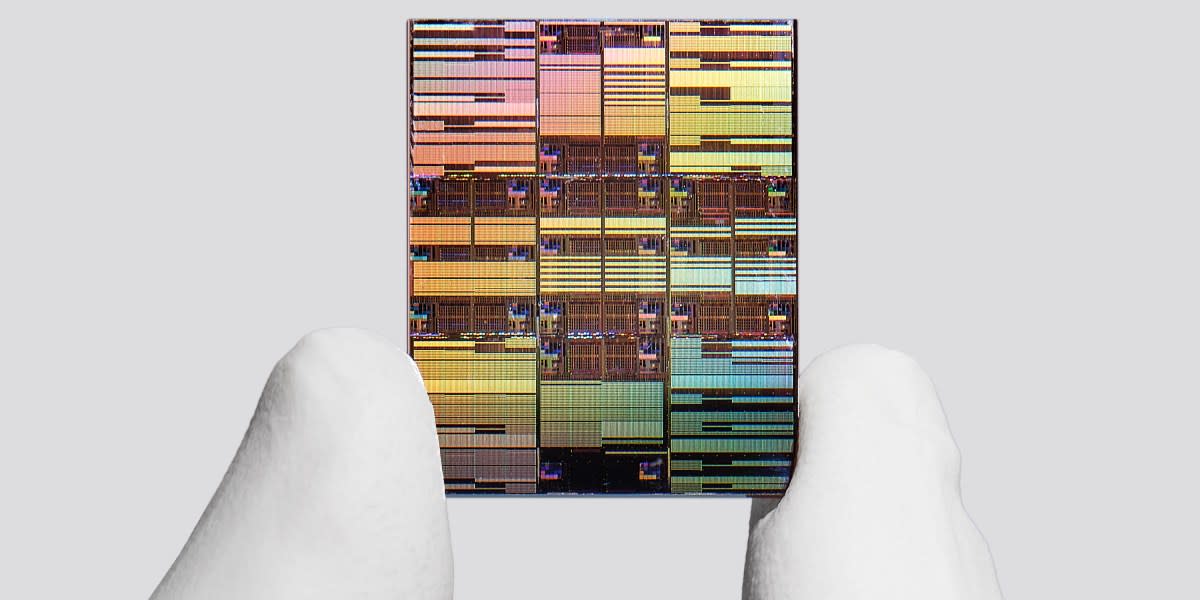
The company unveiled a prototype chip this week that packs around 100 billion transistors onto a fingernail-sized space. That's twice as many as their best chip from just three years ago. The secret? Stacking transistors in two layers like a cake instead of spreading them flat.
The new design, called nanostack technology, works by fabricating one layer of transistors on silicon, then placing another silicon layer on top and building a second set of transistors directly above. Finally, engineers create electrical connections between the two layers. Think of it like city planners building upward when they run out of ground space.
The performance gains are real. Chips using this approach can do 50% more work in the same amount of time compared to IBM's previous best design. They're also up to 70% more energy efficient, which matters enormously for data centers that consume massive amounts of electricity.
Jay Gambetta, director of IBM Research, calls it "a meaningful leap forward" rather than just an incremental step. Within a decade, he expects chips with nanostacking will be standard in data centers worldwide.
What makes IBM's approach special is how the transistors are arranged. The second layer sits staggered rather than directly on top of the first layer, which simplifies the wiring and improves performance. The precision matters because these transistors are incredibly tiny. Each channel inside consists of three nanosheets that are only 15 atoms thick.
The company isn't working alone. Intel, Samsung, and TSMC are all investigating similar vertical stacking approaches. IBM will partner with semiconductor manufacturers to turn this prototype into actual products, including the GPUs and CPUs that power everything from smartphones to artificial intelligence.
The Ripple Effect
This breakthrough arrives at a crucial moment. The world's hunger for computing power keeps growing, especially with the rise of artificial intelligence and machine learning. But making chips more powerful while keeping energy consumption in check has become one of technology's biggest challenges.
Dan Hutcheson, vice chair of technology analysis company TechInsights, calls the development "transformational." He believes it adds another 10 to 15 years to the roadmap for improving computer chips. That means faster smartphones, more powerful laptops, and data centers that can handle increasing demands without burning through electricity.
The technology could help tackle one of computing's thorniest problems: doing more with less energy. As more of our lives move online and AI becomes more prevalent, finding ways to make chips more efficient isn't just good for tech companies. It's good for the planet.
IBM's innovation shows that when one path forward closes, smart engineering can open another. The age of more powerful computers isn't over yet.
Based on reporting by MIT Technology Review
This story was written by BrightWire based on verified news reports.
Spread the positivity!
Share this good news with someone who needs it