IBM's New Chip Tech Offers 50% More Speed, 70% Less Power
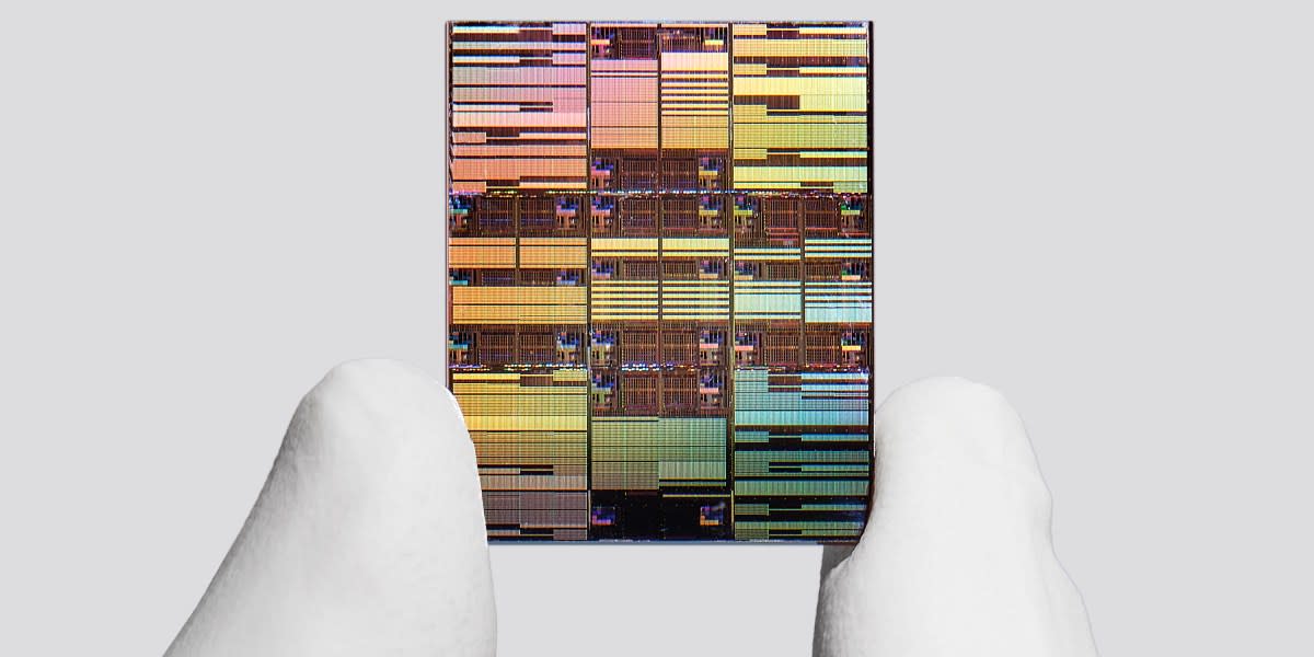
IBM just unveiled breakthrough chip technology that could deliver 50% better performance while slashing energy use by 70%, potentially solving one of AI's biggest problems. The innovation stacks transistors like layers of a cake instead of spreading them flat, cramming nearly 100 billion switches onto a fingernail-sized chip.
The tech industry just got a glimpse of how computers might run cooler, faster, and greener in the very near future.
IBM announced Thursday a major semiconductor breakthrough that could transform everything from smartphones to artificial intelligence data centers. The company's new chip design packs nearly 100 billion transistors onto a fingernail-sized processor, almost double the density of today's cutting-edge technology.
The secret lies in something IBM calls "nanostack." Instead of arranging transistors side by side on a flat surface, the new design stacks them vertically in three-dimensional layers, like floors in a building. This simple shift in architecture unlocks massive gains in both speed and efficiency.
The numbers tell an impressive story. IBM projects these chips could deliver up to 50% better performance than their current 2-nanometer designs. Even more remarkably, they could reduce energy consumption by 70%, a game-changer as AI applications strain power grids worldwide.
Communities near data centers have raised growing concerns about electricity demands. A single large AI training session can consume as much power as hundreds of homes use in a year. Technology that delivers more computing punch while sipping less energy addresses one of the industry's most pressing challenges.
The breakthrough also delivers a 40% improvement in SRAM memory chips, something IBM's vice president of semiconductors Huiming Bu called unprecedented in decades. These memory chips function like a processor's working memory, critical for everything from gaming consoles to laptops.
Taiwan's TSMC, the world's leading chip manufacturer, recently began mass-producing 2-nanometer chips. IBM's 0.7-nanometer technology leaps well beyond that milestone, though the measurement refers to transistor density rather than literal size.
The technology won't hit production lines immediately. IBM expects manufacturing to begin within five years, and the company doesn't make chips itself. Instead, it licenses designs to partners like Japan's Rapidus, which is working to scale up 2-nanometer production.
The Ripple Effect
This advancement arrives at a crucial moment. Artificial intelligence tools like ChatGPT demand enormous computing resources, pushing existing chip technology to its limits. More efficient processors could make AI more accessible while reducing its environmental footprint.
The benefits extend far beyond data centers. Faster, more efficient chips could mean smartphones that last days between charges, laptops that never overheat, self-driving cars with quicker reaction times, and AI assistants that respond instantly while drawing minimal power.
Jay Gambetta, director of IBM Research, captured the significance perfectly: "We're not just making smaller transistors, we're reinventing how chips are built to deliver dramatically more power and energy efficiency."
The race continues, with TSMC developing 1.4-nanometer technology targeted for 2028. But IBM's nanostack approach suggests the path forward isn't just about shrinking components, it's about thinking in three dimensions.
More Images


Based on reporting by Google News - Tech Breakthrough
This story was written by BrightWire based on verified news reports.
Spread the positivity!
Share this good news with someone who needs it