Scientists Create Switchable Diodes From Twisted Crystals
Researchers developed a new way to sculpt 3D electronic devices from single crystals, creating tiny twisted structures that control electricity in both directions. The breakthrough could lead to smaller, more efficient electronics that use shape itself as a design tool.
Scientists just figured out how to make electronics do something new by literally twisting them into shape.
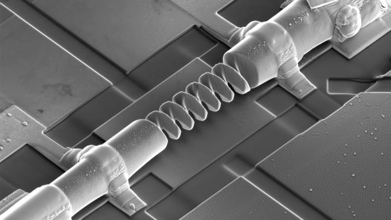
Researchers at Japan's RIKEN Center for Emergent Matter Science created a method to carve three-dimensional devices from single crystal materials at the nanoscale. Using a focused ion beam that cuts with extreme precision, they sculpted tiny helical structures from a magnetic crystal made of cobalt, tin, and sulfur.
The twisted devices work like switchable diodes, letting electric current flow more easily in one direction. What makes them special is that researchers can flip which direction works better by changing the device's magnetization or reversing the helix's twist.
The team proved that the physical shape of a component directly influences how electricity moves through it. By comparing helices of different sizes at various temperatures, they traced the effect to how electrons scatter along the curved, chiral walls of the devices.
This discovery opens the door to electronics built with complex three-dimensional shapes instead of today's flat chips. Those future devices could be smaller, more efficient, and more powerful than what we use now.
Until now, creating 3D nanoscale devices has been challenging. Most fabrication methods limit which materials scientists can use and often compromise the quality of the final product. The new focused ion beam technique works with nearly any crystalline material, giving researchers far more options.
The Ripple Effect spreads across multiple technologies. Diodes are essential components in modern electronics, showing up in AC/DC conversion, signal processing, and LED devices. Shape-engineered components could transform future memory storage, computer logic, and sensor technologies while using less power.
The research team also discovered the interaction works both ways. Strong electrical pulses could flip the magnetization of the twisted structures, suggesting potential applications in data storage where information gets written and read through shape-controlled electrical effects.
Lead researcher Max Birch explained that treating geometry as a design tool puts it on equal footing with the intrinsic properties of materials themselves. The nanosculpting method opens up studies on how 3D and curved device shapes can create entirely new electronic functions.
The convergence of materials physics and nanofabrication points toward functional device designs that weren't possible before. By combining the natural properties of advanced materials with engineered curvature, researchers can explore electronic behaviors that only happen when electricity flows through precisely shaped pathways at tiny scales.
This breakthrough shows that sometimes the solution isn't just finding better materials but learning to shape the ones we have in smarter ways.
Based on reporting by Science Daily
This story was written by BrightWire based on verified news reports.
Spread the positivity!
Share this good news with someone who needs it