Singapore Builds AI Materials Hub for Chip Innovation
Singapore is launching a groundbreaking materials innovation center that combines AI and advanced atomic processing to speed up semiconductor breakthroughs. The new hub aims to make Singapore a global leader in next-generation manufacturing.
Singapore just took a major leap forward in becoming a powerhouse for advanced materials and semiconductor innovation.
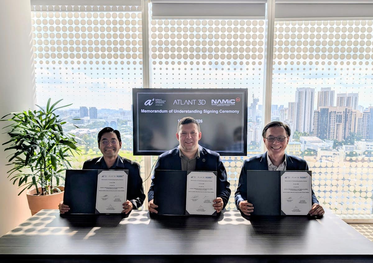
ATLANT 3D, a Danish technology company, has partnered with two leading Singapore research organizations to create the Advanced Materials Development Hub, or A-HUB. The collaboration brings together cutting-edge atomic layer processing technology with world-class materials science expertise and manufacturing capabilities.
The new hub will focus on discovering and developing materials for semiconductors, silicon photonics, and advanced chip packaging. Using AI-driven techniques, researchers will be able to test and create new materials much faster than traditional methods allow.
At the heart of the collaboration is ATLANT 3D's Direct Atomic Layer Processing technology, which enables precise material creation at the atomic level. This will be combined with the Institute of Materials Research and Engineering's deep materials science knowledge and the National Additive Manufacturing Innovation Cluster's innovation ecosystem.
The timing couldn't be better. As global demand for advanced chips continues to surge, finding new materials with superior properties has become critical for next-generation electronics. A-HUB aims to bridge the gap between laboratory discoveries and real-world manufacturing applications.
The Ripple Effect
This partnership strengthens Singapore's position as a global manufacturing and innovation hub while creating opportunities for industry partners to access cutting-edge research capabilities. The high-throughput approach means materials that once took years to develop could be created in months.
The hub will also support Singapore's sovereign manufacturing infrastructure, reducing dependence on external sources for critical materials technology. By bringing together research institutions, technology companies, and industry partners under one roof, A-HUB creates a shared platform for accelerating breakthrough discoveries.
Dr. Maksym Plakhotnyuk, CEO of ATLANT 3D, describes the initiative as creating "the world's first high-throughput materials innovation foundry" for advanced semiconductor applications. Professor Loh Xian Jun from A*STAR IMRE emphasized how the collaboration will translate research into practical outcomes for Singapore's advanced manufacturing industry.
Singapore's track record in industrial-scale adoption of advanced technologies makes it an ideal location for this ambitious project. The nation has consistently invested in building world-class research infrastructure and attracting global technology partnerships.
A-HUB represents more than just a research facility—it's a blueprint for how collaboration between international tech companies and national research institutions can accelerate innovation that benefits everyone.
More Images


Based on reporting by Google News - Singapore Technology
This story was written by BrightWire based on verified news reports.
Spread the positivity!
Share this good news with someone who needs it