IBM Unveils 0.7nm Chip That Fits 100 Billion Transistors
IBM just announced the world's smallest chip technology at 0.7 nanometers, packing 100 billion transistors into a space the size of your fingernail. This breakthrough could slash AI training time from three months to just two weeks.
IBM just became the first company to break the 1-nanometer barrier in chip technology, unveiling a 0.7-nanometer manufacturing process that could transform everything from smartphones to artificial intelligence.
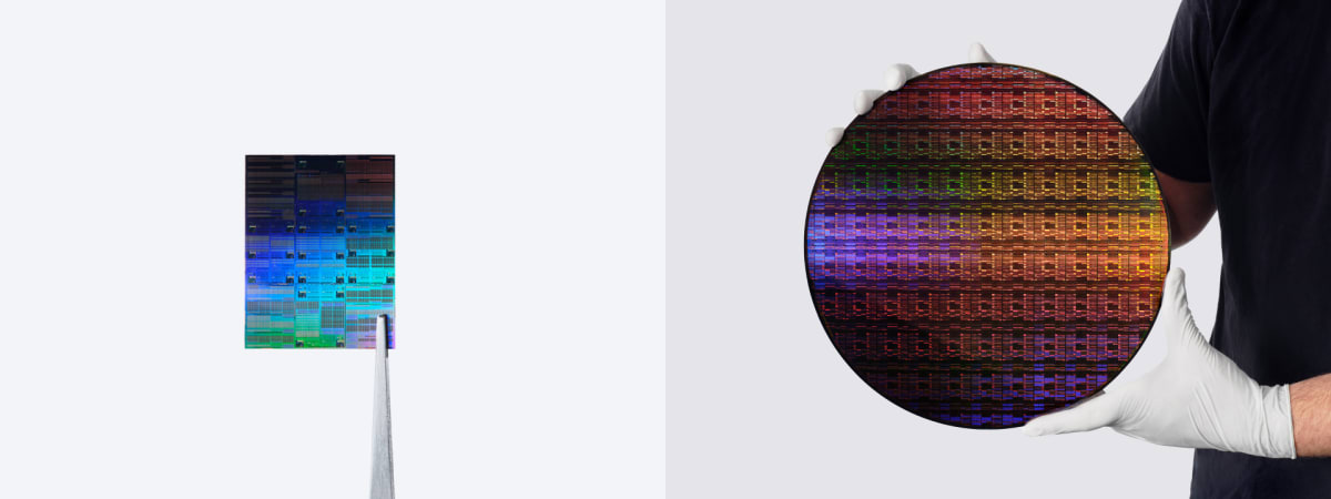
The breakthrough centers on IBM's new "nanostack" technology, which vertically stacks and staggers transistors like a microscopic high-rise building. This 3D approach allows engineers to pack an astonishing 100 billion transistors onto a chip the size of a fingernail.
The numbers tell an exciting story. Compared to IBM's 2-nanometer chips from 2021, these new processors deliver either 70% better power efficiency or 50% more performance. For everyday users, that could mean smartphones that last days on a single charge or laptops that run intensive programs without breaking a sweat.
But the real game-changer shows up in artificial intelligence. IBM says an AI chip built with this technology could reach 9,000 trillion operations per second, double the current 4,500 TOPS benchmark. That leap would cut AI model training time from three months down to just a couple of weeks.
The technology builds on IBM's earlier nanosheet innovation, which laid flat sheets of semiconductor material to create transistors. The new nanostack method takes that concept vertical, stacking these sheets in three dimensions. IBM validated the approach by developing a new wafer-bonding technique that requires precision alignment at the atomic level.
While Taiwan's TSMC has also explored nanosheet technology, IBM's vertical stacking approach represents a distinct evolution. The company demonstrated that its ultra-thin dielectric bonding works in actual chip integration, not just laboratory conditions.
The Ripple Effect
This advancement reaches far beyond faster phones. More efficient chips mean data centers that consume less energy, reducing the environmental impact of our digital world. AI researchers could test and refine models in weeks instead of months, accelerating breakthroughs in medicine, climate science, and beyond.
The technology also signals strength in American semiconductor innovation at a crucial moment. As global demand for advanced chips continues growing, homegrown breakthroughs like this reinforce domestic manufacturing capabilities and research leadership.
Manufacturing chips this small requires solving enormous technical challenges, from atomic-level precision to managing heat in microscopic spaces. IBM's success proves these obstacles aren't insurmountable.
The path from research lab to mass production typically takes years, but this announcement shows the roadmap ahead for next-generation computing is getting clearer every day.
More Images


Based on reporting by Google News - Innovation Technology
This story was written by BrightWire based on verified news reports.
Spread the positivity!
Share this good news with someone who needs it