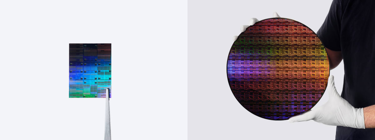
IBM's 0.7nm Chip Packs 666 Million Transistors Per mm²
IBM just cracked the code on impossibly tiny computer chips that could make your future phone five times more powerful while using half the energy. The breakthrough, called NanoStack, stacks transistors like LEGO blocks instead of laying them flat.
The future of computing just got a whole lot smaller, and that's fantastic news for everyone who's ever wished their phone battery lasted longer or their laptop ran faster.
IBM researchers have achieved something the tech world thought was still years away. They've successfully built working computer chips using a revolutionary 0.7-nanometer process that crams 666 million transistors into a space smaller than a grain of sand.
To put that in perspective, if IBM's previous chips were city blocks, these new ones are skyscrapers. The company managed this by fundamentally rethinking how transistors are arranged, stacking them vertically instead of spreading them across a flat surface.
The technology, branded as NanoStack, delivers numbers that sound almost too good to be true. Chips built with this process use 50% less space, run 50% faster at the same power level, or achieve 70% better efficiency at the same speed. Memory components also shrink by 40%, meaning more storage in smaller devices.
IBM achieved this milestone by being the first to successfully build what's called a CFET, or Complementary FET transistor. Think of it as the difference between building a ranch house versus a tower. Previous chip designs had hit a wall because you can only squeeze so many transistors side by side before physics says no.
The breakthrough follows IBM's 2021 achievement when they became the first to demonstrate Gate-All-Around transistors, a design that's only now hitting the market in 2026. While IBM doesn't manufacture consumer chips itself, its research paves the way for companies that do.
The Ripple Effect
This isn't just about faster phones, though that's certainly coming in about five years when the technology reaches market. More efficient chips mean longer battery life for medical devices, more powerful AI that can run on smaller hardware, and data centers that consume less energy while doing more work.
The environmental impact matters too. As our world runs on more computing power, making chips that do more with less energy directly reduces the carbon footprint of our digital lives.
IBM's willingness to share its research has already accelerated the entire industry. Their 2021 breakthrough inspired similar designs from Samsung, Intel, and TSMC that are powering devices today. This new leap forward will likely do the same, creating a wave of innovation across the tech sector.
The Albany NanoTech facility where IBM conducted this research is also installing a High-NA EUV machine, the most advanced chip-making tool available, which will help refine the process even further.
In a world where some experts declared Moore's Law dead, IBM just proved there's still plenty of room to grow by thinking in three dimensions instead of two.
More Images


Based on reporting by Google News - Business
This story was written by BrightWire based on verified news reports.
Spread the positivity!
Share this good news with someone who needs it