MIT Creates Bendable, See-Through Computer Chips
Scientists at MIT have figured out how to make computer chips you can bend and see through, opening doors to health monitors that wrap around your body and clear augmented reality displays. The breakthrough works at factory scale, meaning these flexible chips could soon move from lab experiments to real-world products.
Imagine a health monitor so thin and flexible it moves with your skin, or augmented reality displays so clear they're nearly invisible on a pilot's helmet visor.
MIT researchers just made that future possible by creating the first factory-scale process for making computer chips that bend without breaking and let light pass right through them. Unlike previous lab experiments that could only make a few devices at a time, this new method produces full-sized wafers using standard manufacturing equipment.
The innovation centers on silicon photonics, a technology that uses light instead of electricity to move and process information. Until now, these advanced chips have been rigid and opaque, limiting where they could be used.
Working with engineers at NY Creates in Albany, the MIT team developed a process that starts like traditional chip making but adds clever new steps. They build the chip's light-carrying components on a standard silicon wafer, then carefully flip and remove layers until only the essential parts remain, thinner than a tenth of a human hair.
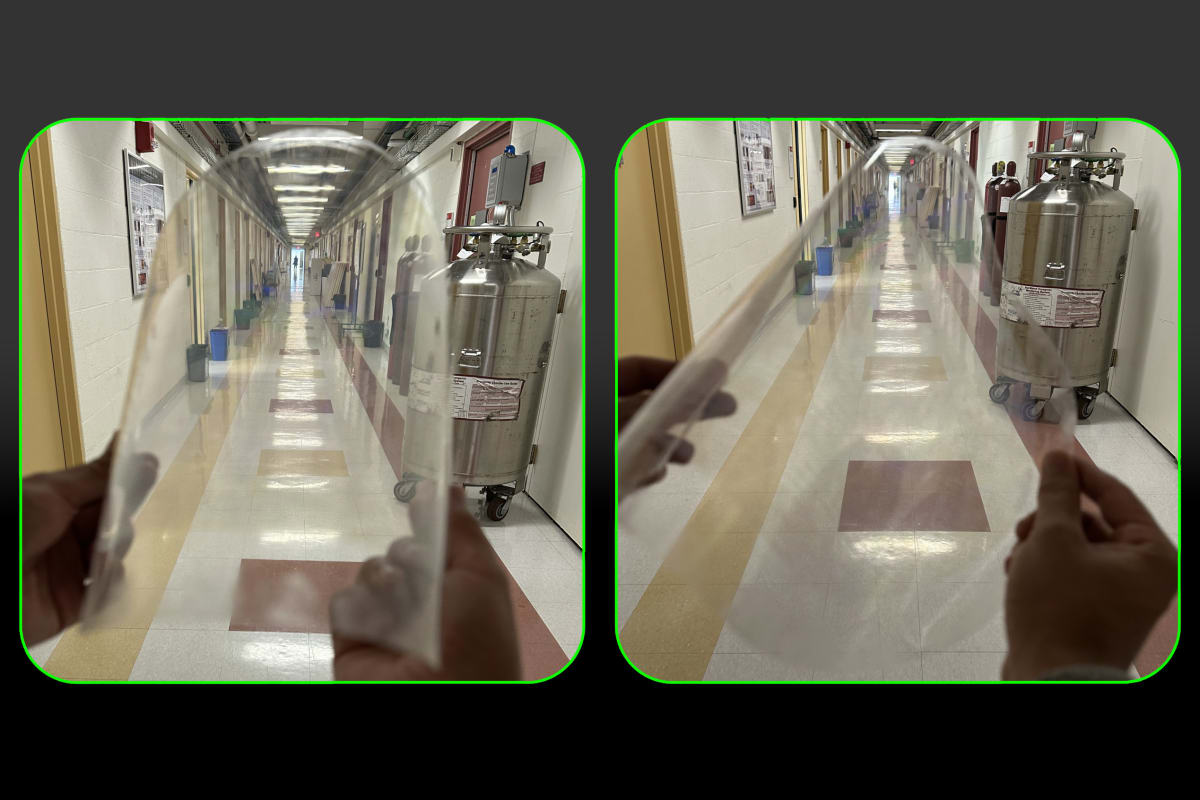
The final product gets bonded to a transparent polyester film just a few microns thick. The result is a flexible, see-through wafer containing billions of nanoscale optical devices that work just as reliably as their rigid counterparts.
To prove the chips could handle real-world use, researchers bent a single chip thousands of times around cylinders as narrow as a small screw. Performance never dropped. They also confirmed that looking through the chips causes minimal distortion or haze.
The Ripple Effect
This breakthrough could transform how we interact with technology in our daily lives. Doctors could use conformable health sensors that stick comfortably to skin for continuous monitoring. Pilots and drivers might get critical information displayed on transparent, curved screens that match their field of vision perfectly.
Because the process uses standard 300-millimeter foundry equipment, manufacturers can produce these chips with the same reliability and scale as conventional silicon chips. That means designers can confidently create complex systems with billions of components, knowing they'll all work as intended.
The MIT team plans to make their platform available to other research groups, potentially accelerating development across the entire silicon photonics field. Opening access could spark innovations nobody has imagined yet.
Lead researcher Jelena Notaros, an associate professor of electrical engineering at MIT, sees this as unlocking application areas that simply weren't possible before. The combination of flexibility and transparency creates opportunities that neither property alone could achieve.
The technology represents years of careful work pushing manufacturing processes to their limits while keeping costs practical for real products.
Sometimes the biggest breakthroughs come from making existing technology work in ways nobody thought possible.
Based on reporting by MIT News
This story was written by BrightWire based on verified news reports.
Spread the positivity!
Share this good news with someone who needs it