New 0.42nm Interface Breakthrough Could Revolutionize Chips
Scientists solved a decade-old problem blocking the next generation of computer chips by engineering an interface just a fraction of a nanometer thick. The breakthrough lets transistors be smaller and faster without sacrificing performance.
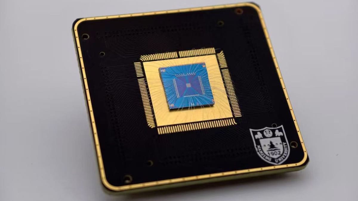
For over ten years, researchers have known that atomically thin materials could transform computing, but a stubborn engineering problem kept blocking progress. Scientists at National Yang Ming Chiao Tung University and TSMC just solved it with an innovation measured in fractions of a nanometer.
The breakthrough centers on transistors, the tiny switches that power every computer chip. As these components shrink, they become faster and more energy efficient, but there's a catch. Modern transistors need an ultrathin insulating layer called a gate dielectric to control electron flow, and adding this layer to atomically thin semiconductors has always caused problems.
Until now, engineers faced an impossible choice. They could make the insulating layer thinner for better electrical control, or they could protect the smooth flow of electrons through the device. Achieving both seemed out of reach because the boundary where materials meet would get disrupted, scattering electrons and killing performance.
Professor Wen-Hao Chang and his team took a completely different approach. Instead of searching for better semiconductor materials, they redesigned the atomic interface itself, the narrow region where two materials meet that's only a few atoms thick.
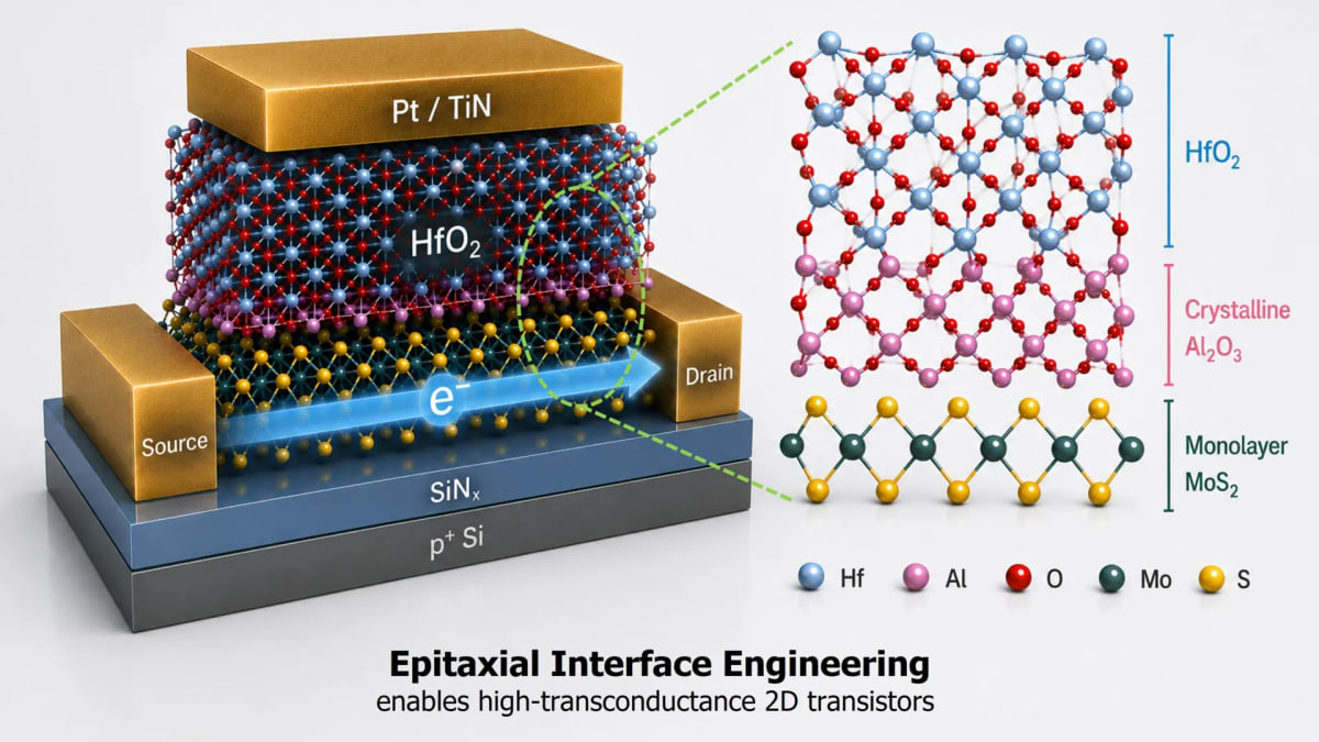
The researchers placed an ultrathin layer of aluminum directly onto molybdenum disulfide, then carefully oxidized it to create an aluminum oxide layer just 0.42 nanometers thick. They added a hafnium oxide gate dielectric on top, and something remarkable happened.
Despite being thinner than a single nanometer, this engineered interface does two critical jobs at once. It creates a smooth surface that lets the insulating layer grow evenly, and it acts as an atomic buffer that protects electrons as they zip through the transistor channel.
The results exceeded expectations. The new transistors showed low leakage current, minimal electrical noise, and strong performance in devices with channels measuring just tens of nanometers. Most importantly, engineers no longer have to choose between electrical control and electron mobility.
The Ripple Effect
This discovery could accelerate the entire semiconductor industry's transition beyond silicon. Manufacturers have spent decades refining silicon technology, but physics imposes hard limits on how much smaller traditional transistors can get.
Atomically thin semiconductors offer a path forward, potentially enabling chips that are smaller, faster, and dramatically more energy efficient than anything possible with silicon alone. The interface breakthrough removes one of the main obstacles that has held back this transition.
The team's focus on the atomic boundary rather than the bulk materials themselves opens new possibilities. Sometimes the biggest leaps forward come not from finding completely different materials, but from perfecting how existing ones work together.
The future of computing might be measured in fractions of nanometers.
Based on reporting by Science Daily
This story was written by BrightWire based on verified news reports.
Spread the positivity!
Share this good news with someone who needs it