MIT's AI Detects Six Hidden Defects in Materials at Once
Engineers can now see invisible atomic flaws in semiconductors and solar cells without destroying them, thanks to a breakthrough AI model from MIT. The technology could make everything from computer chips to batteries more reliable and efficient.
Scientists just solved a puzzle that's been frustrating engineers for decades: how to measure the tiny imperfections in materials that make them work better.
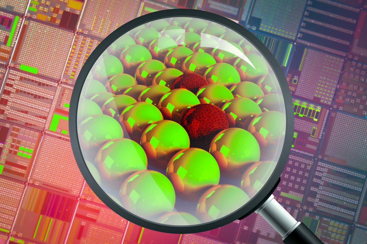
MIT researchers built an AI model that can spot up to six different atomic defects in materials like semiconductors and solar cells simultaneously. It's the first tool that can do this without cutting open or damaging the finished product.
Here's why that matters. In materials science, defects aren't always bad. Manufacturers deliberately introduce microscopic flaws into steel, computer chips, and solar panels to make them stronger, conduct electricity better, or convert energy more efficiently. But until now, they've been flying blind about what defects actually ended up in their finished products.
"Engineers have many ways to introduce defects, but they still struggle with basic questions like what kind of defect they've created and in what concentration," says postdoc Chu-Liang Fu. Without knowing what's inside, companies risk making products that perform poorly or behave unexpectedly.
The MIT team trained their model on 2,000 different semiconductor materials using neutron scattering, a technique that measures how atoms vibrate. The AI learned to spot the difference between materials with and without defects, then predict exactly which imperfections exist and how many.
Lead author Mouyang Cheng, a PhD candidate, explains that conventional techniques can only see part of the picture. Some methods identify defect types but not quantities. Others require destroying the material to examine it. "Detecting six different defects is unthinkable with conventional techniques," he says. "It's something you can't do any other way."
The researchers tested their model on electronics alloys and superconductor materials. It successfully detected defect concentrations as low as 0.2 percent, a level of precision that opens new possibilities for quality control.
The Ripple Effect
This breakthrough could transform how we make the technology powering modern life. Semiconductor manufacturers could fine-tune computer chips with greater precision. Solar panel makers could optimize energy conversion more reliably. Battery producers could engineer materials that store power more efficiently and safely.
The model covers 56 elements in the periodic table, giving it broad applications across industries. Senior author Mingda Li, an associate professor of nuclear science and engineering, says the technology helps scientists finally see "the full elephant" instead of just isolated parts.
The research appears in the journal Matter and represents years of work applying machine learning to materials science. The team used attention mechanisms similar to those in ChatGPT to extract meaningful patterns from complex spectroscopy data.
For an industry that's been guessing about what's inside their products, having a reliable map of defects means fewer failures, better performance, and faster innovation in the technologies we depend on every day.
Based on reporting by MIT News
This story was written by BrightWire based on verified news reports.
Spread the positivity!
Share this good news with someone who needs it